(China (Mainland))

Product Summary
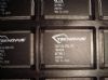
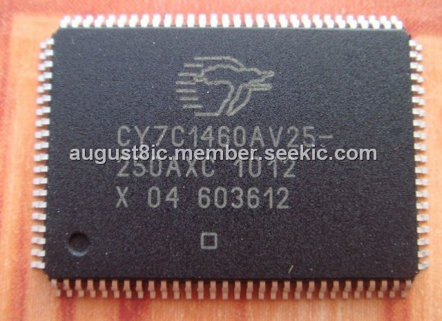
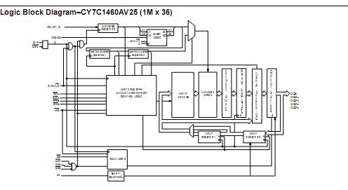
The CY7C1460AV25-250AXC is a 2.5V, 1M x 36/2M x 18/512 x 72 Synchronous pipelined burst SRAM with No Bus Latency (NoBL) logic, respectively. The CY7C1460AV25-250AXC is designed to support unlimited true back-to-back Read/Write operations with no wait states. The CY7C1460AV25-250AXC is equipped with the advanced (NoBL) logic required to enable consecutive Read/Write operations with data being transferred on every clock cycle.
Parametrics
CY7C1460AV25-250AXC absolute maximum ratings: (1) Storage Temperature: -65 to +150°C; (2) Ambient Temperature with Power Applied: -55 to +125°C; (3) Supply Voltage on VDD Relative to GND: -0.5 to +3.6V; (4) Supply Voltage on VDDQ Relative to GND: -0.5 to VDDQ +0.5V; (5) DC to Outputs in Tri-State: -0.5 to VDD +0.5V; (6) Current into Outputs (LOW) : 20mA; (7) Current into Outputs (LOW) : > 2001V; (8) Latch-up Current: > 200mA.
Features
CY7C1460AV25-250AXC features: (1) Pin-compatible and functionally equivalent to ZBT; (2) Supports 250-MHz bus operations with zero wait states; (3) nternally self-timed output buffer control to eliminate the need to use asynchronous OE; (4) Fully registered (inputs and outputs) for pipelined operation; (5) 2.5V core power supply; (6) ) Clock Enable CEN pin to suspend operation; (7) Synchronous self-timed writes; (8) Burst capability-linear or interleaved burst orde.
Diagrams
| Image | Part No | Mfg | Description |  |
Pricing (USD) |
Quantity | ||||||||||
|---|---|---|---|---|---|---|---|---|---|---|---|---|---|---|---|---|
 |
 CY7C1460AV25-250AXC |
Cypress Semiconductor |
SRAM 1Mx36 2.5V NoBL PL SRAM COM |
Data Sheet |
|
|
||||||||||
 |
CY7C1460AV25-250AXCT |
|
IC SRAM 36MBIT 250MHZ 100LQFP |
Data Sheet |
Negotiable |
|
||||||||||