Product Summary
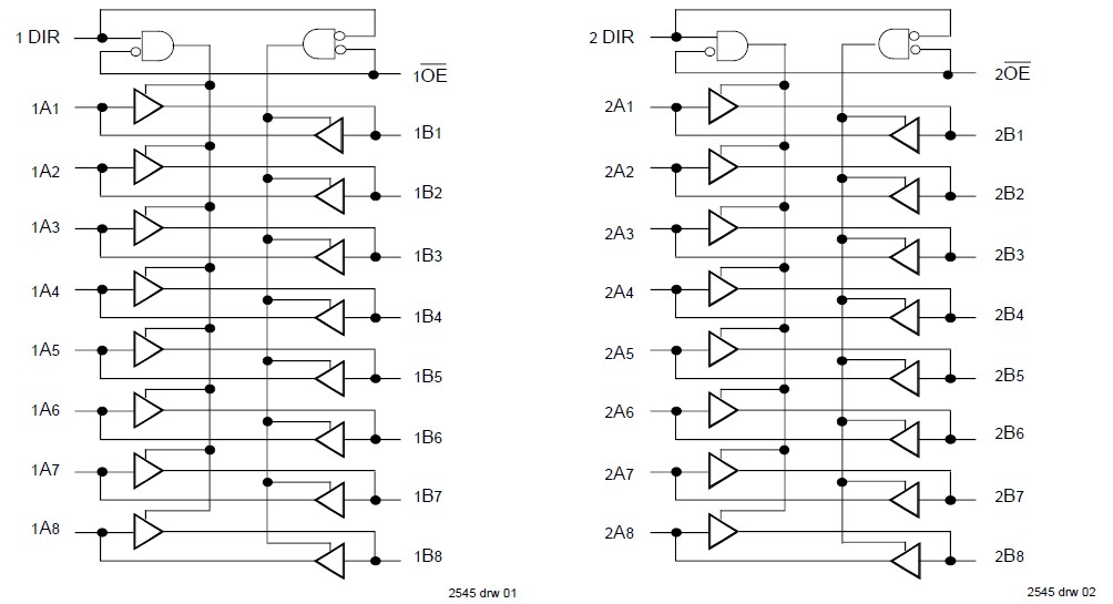
The IDT74FCT16245ATPV is a 16-bit transceiver. The IDT74FCT16245ATPV is built using advanced dual metal CMOS technology. The IDT74FCT16245ATPV is ideal for synchronous communication between two busses (A and B). The Direction and Output Enable controls operate these devices as either two independent 8-bit transceivers or one 16-bit transceiver. The direction control pin (xDIR) controls the direction of data flow. The output enable pin (xOE) overrides the direction control and disables both ports. All inputs are designed with hysteresis for improved noise margin.
Parametrics
IDT74FCT16245ATPV absolute maximum ratings: (1)VTERM Terminal Voltage with Respect to GND: –0.5 to +7.0 V; (2)VTERM Terminal Voltage with Respect to GND: –0.5 to VCC +0.5 V; (3)TSTG Storage Temperature: –65 to +150 °C; (4)IOUT DC Output Current: –60 to +120 mA.
Features
IDT74FCT16245ATPV features: (1)0.5 MICRON CMOS Technology; (2)High-speed, low-power CMOS replacement for ABT functions; (3)Typical tSK(o)(Output Skew)< 250ps; (4)Low input and output leakage £ 1mA (max.); (5)ESD > 2000V per MIL-STD-883, Method 3015; > 200V using machine model (C = 200pF, R = 0); (6)Packages include 25 mil pitch SSOP, 19.6 mil pitch TSSOP, 15.7 mil pitch TVSOP and 25 mil pitch Cerpack; (7)Extended commercial range of -40°C to +85°C; (8)High drive outputs (-32mA IOH, 64mA IOL); (9)Power off disable outputs permit “live insertion”; (10)Typical VOLP (Output Ground Bounce)< 1.0V at VCC = 5V, TA = 25°C; (11)Balanced Output Drivers: ±24mA (commercial), ±16mA (military); (12)Reduced system switching noise; (13)Typical VOLP (Output Ground Bounce)< 0.6V at VCC = 5V,TA = 25°C.
Diagrams

| Image | Part No | Mfg | Description |  |
Pricing (USD) |
Quantity | ||||||||||||||||||||||
|---|---|---|---|---|---|---|---|---|---|---|---|---|---|---|---|---|---|---|---|---|---|---|---|---|---|---|---|---|
 |
 IDT74FCT16245ATPVG |
 |
 IC TRANSCVR BIDIR 16BIT 48TSSOP |
 Data Sheet |

|
|
||||||||||||||||||||||
 |
 IDT74FCT16245ATPVG8 |
 |
 IC BI-DIRECT TRSCVR 16BIT 48SSOP |
 Data Sheet |

|
|
||||||||||||||||||||||
 (China (Mainland))


