(China (Mainland))

Product Summary
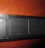
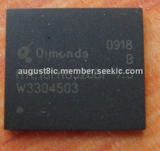
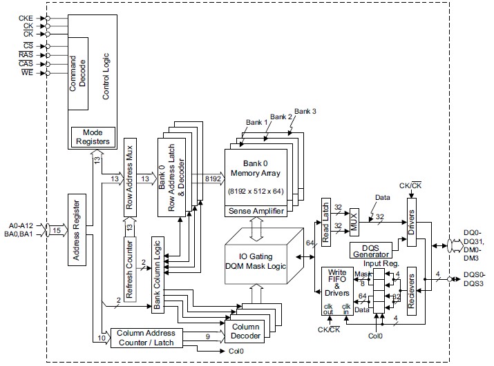
The HYE18M1G320BF-7.5 is a high-speed CMOS, dynamic random-access memory containing 1,073,741,824 bits. The HYE18M1G320BF-7.5 is internally configured as a quad-bank DRAM. The HYE18M1G320BF-7.5 uses a double-data-rate architecture to achieve high-speed operation. The double-data-rate architecture is essentially a 2n pre fetch architecture, with an interface designed to transfer two data words per clock cycle at the I/O balls. A single READ or WRITE access for the DDR Mobile-RAM consists of a single 2n-bit wide, one clock cycle data transfer at the internal DRAM core and two corresponding n-bit wide, one-half clock cycle data transfers at the I/O balls.
Parametrics
HYE18M1G320BF-7.5 absolute maximum ratings: (1)Power Supply Voltage VDD: -0.3 to 2.7 V; (2)Power Supply Voltage for Output Buffer VDDQ: -0.3 to 2.7 V; (3)Input Voltage VIN: -0.3 to VDDQ + 0.3 V; (4)Output Voltage VOUT: -0.3 to VDDQ + 0.3 V; (5)Operating Case Temperature Commercial TC: 0 to +70 ℃; (6)Extended TC: -25 to +85 ℃; (7)Storage Temperature TSTG: -55 to +150 ℃; (8)Power Dissipation PD: 0.7 W; (9)Short Circuit Output Current IOUT: 50 mA.
Features
HYE18M1G320BF-7.5 features: (1)Low power DDR 1Gbit x32 dual die implementation; (2)Each die is organized as 4 banks x 8 Mbit x16; (3)Double-data-rate architecture: two data transfers per clock cycle; (4)Bidirectional data strobe (DQS)is transmitted / received with data; to be used in capturing data at the receiver; (5)DQS is edge-aligned with data for READs and center-aligned with data for WRITEs; (6)Differential clock input (CK / CK); (7)Commands entered on positive CK edge; data and mask data are referenced to both edges of DQS; (8)Four internal banks for concurrent operation; (9)Programmable CAS latency: 2 and 3; (10)Programmable burst length: 2, 4, 8 and 16; (11)Programmable drive strength (full, half, quarter); (12)Auto refresh and self refresh modes; (13)8192 refresh cycles / 64ms; (14)Auto precharge; (15)Commercial (-0℃ to +70℃)and Extended (-25℃ to +85℃)operating temperature ranges; (16)90-ball PG-VFBGA-90-5 package (11 × 12.5 × 1.0 mm).
Diagrams
 |
 HYE18P32161AC-L85 |
Other |
|
Data Sheet |
Negotiable |
|
||||
|
HYE18P32161AC-L70 |
Other |
|
Data Sheet |
Negotiable |
|
||||
|
HYE18P32161AC-85 |
Other |
|
Data Sheet |
Negotiable |
|
||||
|
HYE18P32161AC-70 |
Other |
|
Data Sheet |
Negotiable |
|
||||
|
HYE18P32160AC9.6 |
Other |
|
Data Sheet |
Negotiable |
|
||||
|
HYE18P32160AC15 |
Other |
|
Data Sheet |
Negotiable |
|
||||